内置频率调节32.768 kHz晶体单元,符合AEC-Q200
接口类型:4线串行接口;宽工作电压范围:1.6V to 5.5V
宽计时器电压范围:1.5V to 5.5V,Ta=-40°C to +125°C
扩展工作温度范围:-40°C to +125°C
32.768 kHz时钟/日历功能,自动闰年校正功能
应用领域:汽车音频、汽车导航系统、时钟、ECU子时钟
RA-4565SA(AEC-Q200): 爱普生(EPSON) 汽车用串行接口实时时钟模块,实时时钟芯片RTC
完整型号:
型号 | 料号 | 封装 | MOQ |
RA-4565SA | Q41A46552xxxx00 | SOP-14 | 1000PCS/Reel |
RA-4565SA B | Q41A46552xxxx00 | SOP-14 | 1000PCS/Reel |
RA-4565SA 特征
• 内置频率调节32.768 kHz晶体单元。
• 接口类型:4线串行接口
• 宽工作电压范围:1.6V to 5.5V
• 宽计时器电压范围:1.5V to 5.5V,Ta=-40°C to +125°C
• 扩展工作温度范围:-40°C to +125°C
• 32.768 kHz时钟/日历功能,自动闰年校正功能
• 应用领域:汽车音频、汽车导航系统、时钟、ECU子时钟
• 符合AEC-Q200
RA-4565SA 概述
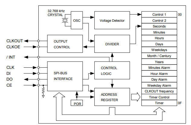
该模块芯片RA-4565SA是具有4线形式(或3线形式)串行接口的实时时钟芯片。它有一个内置的晶体振荡器。工作温度范围为−40°C至+125°C,适用于汽车附件。除了日历(年、月、日、工作日、小时、分钟、秒)功能和时钟计数器功能外,该模块的实时时钟功能还包括报警功能和固定周期计时器中断功能。
• 宽工作温度范围:-40°C至+125°C
• 时钟状态检测功能
它可以通过VL位的状态来判断备份操作返回后数据的有效性。
• 32.768 kHz频率输出功能
CLKOUT引脚输出(漏极开路输出)
输出频率可选择为32.768 kHz、1024 Hz、32 Hz或1 Hz。
• 各种中断功能
定时器功能可设置在1/4096秒和255分钟之间。
RA-4565SA 系统框图
推荐操作条件(Recommend Operating Conditions)
Item | Symbol | Conditions | Min. | Typ. | Max. | Unit |
Operating voltage | VDD | - | 1.6 | 3.0 | 5.5 | V |
Timekeeper voltage | VCLK | - | 1.5 | 3.0 | 5.5 | V |
Operating temperature | TOPR | - | -40 | +25 | +125 | °C |
频率特性(Frequency characteristics)
Item | Symbol | Conditions | Rating | Unit |
Frequency stability | Δ f/f | Ta=+25°C VDD=3.0V | 5±23 *1 | ×10-6 |
Oscillation start up time | tSTA | Ta=+25°C VDD=1.6V | 1.5 Max. | s |
Ta = -40°C to +125°C VDD=3.0V | 3.0 Max. | s |
*1 ) Equivalent to ±1 minutes of monthly deviation.
备份模式下的功耗(Current consumption under backup mode.)
Item | Symbol | Conditions | Min. | Typ. | Max. | Unit | |
Standby current. | lBK | fSCL = 0 Hz | +125°C | 1.0 | 2.0 | µA | |
-40 to +85°C | 0.6 | 1.2 | |||||
fSCL = 0 Hz | +125°C | 0.8 | 1.6 | µA | |||
-40 to +85°C | 0.5 | 1.0 | |||||
(1) 产品名称 (标准形式)
Product Name RA-4565SA
RA-4565SA B
(Standard form) ① ② ③
① Model ② Package type (SA : SOP-14pin)
③ Frequency tolerance (Exclude offset):
Blank or B: 5±23 x 10-6 (Equivalent to ± 1 minute of monthly deviation) @ +25°C
(2) 产品型号 / 产品编码 (空白部分由每个详细规范决定。)
RA-4565SA Q41A46552xxxx00
① ② ③ ④ ⑤
① Crystal devices ② Model
③ Pb free code (2: EU RoHS compliant / Terminal plating : Sn)
④ Detail specifications ⑤ Packaging (SA: 1000pcs/Reel)
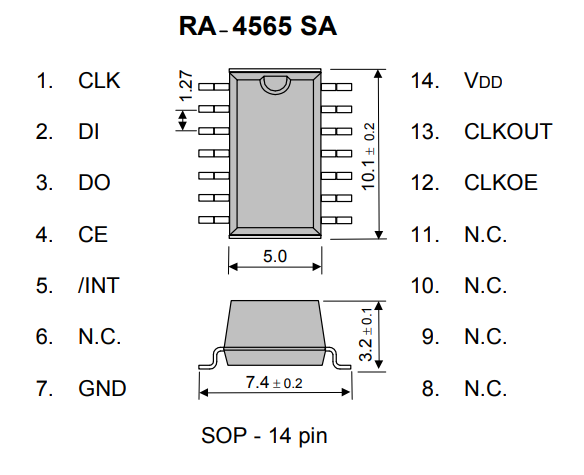
Terminal | Directions | Functions |
CE | Input | Chip enabled input. |
CLK | Input | Serial clock input. |
Dl | Input | Data input. |
DO | Output | Data output. |
CLKOUT | Output | The CLKOUT pin is a clock output(open drain output)pin with control |
CLKOE | Input | |
/INT | Output | Interrupts output by Alarm and Timer events. (Open drain output) |
VDD | - | VDD |
GND | - | GND |
RA-4565SA 外形尺寸 Unit: mm
模塑料内部的金属外壳可能会暴露在本产品的顶部或底部。 这纯粹是装饰性的,对质量、可靠性或电气规格没有任何影响。
RA-4565SA Footprint (Recommended) Unit: mm
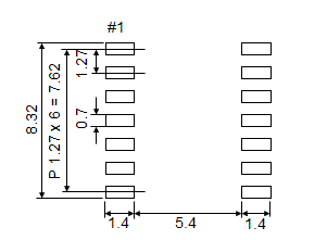
为保持稳定运行,在尽可能靠近晶体产品电源端子的位置(Vcc - GND 之间)需提供一个 0.1uF 的去耦电容。
 在线咨询
在线咨询
 微信服务
微信服务