内置调频32.768 kHz 晶体单元
接口类型:I2C-Bus接口
低备份电流:240 nA 典型值 / 3V
频率输出功能:输出频率可选择32.768kHz、1024Hz、1Hz
自动重复唤醒定时器中断
时间戳功能
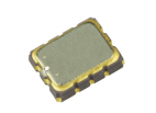
RX8901CE:爱普生(EPSON) 低电流消耗、时间戳功能、高稳定性、I2C总线接口实时时钟芯片
内置32.768 kHz-DTCXO,+105ºC工作温度,低电流消耗,内置电源开关电路和时间戳功能,最多32条记录
完整型号:
型号 | 料号 | 封装 | MOQ |
RX8901CE XS A0 | X1B000481000115 | 3.2 x 2.5 x 1.0 | 2000PCS/REEL |
RX8901CE XB A0 | X1B000481000215 | 3.2 x 2.5 x 1.0 | 2000PCS/REEL |
RX8901CE XS B0 | X1B000481000315 | 3.2 x 2.5 x 1.0 | 2000PCS/REEL |
RX8901CE XB B0 | X1B000481000415 | 3.2 x 2.5 x 1.0 | 2000PCS/REEL |
• 内置频率调整
32.768 kHz 晶体单元
• 接口类型
I2C-Bus接口
• 低备用电流
240 nA 典型值 / 3V
• 自动电源切换功能
通过监控 VDD 电压自动切换到备用电源
• 时间戳功能
最多 32 次 标记从年到 1/1024 秒。
• 时间更新中断
每小时、每分钟和第二次
• 日、日期、时、分、秒的闹铃中断
• 自动重复唤醒定时器中断
• 自我监控中断
晶体振荡停止。
VBAT 低,VDD 低。
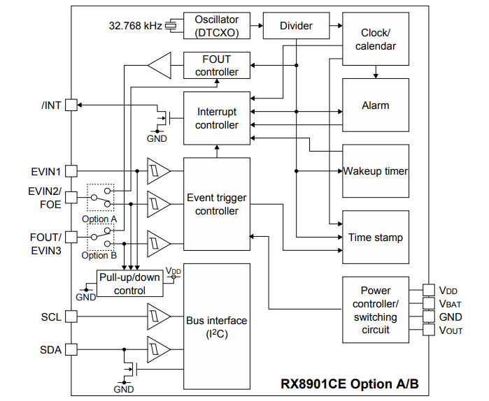
RX8901CE 概述
RX8901CE 是一款集成了 32.768 kHz 数字温度补偿晶体振荡器 (DTCXO) 的 RTC 模块。它包括各种功能,例如当外部或内部事件发生时可记录多达 32 个日期和时间的时间戳功能,以及时间和日历、时间警报、唤醒定时器和时间更新中断等基本 RTC 功能。 RX8901CE 结合了自动电源切换功能,其中包括防止主电源反向电流的控制电路、连续温度校正的 32.768 kHz 时钟生成以及 Seiko Epson 独创的低电流消耗技术,可实现较长的电池寿命在各种系统上。
• 接口类型: I2C-Bus 快速模式 400 kHz
• 高稳定性
XS:±3.0 x 10⁻⁶ / -40 ºC 至 +85 ºC(月费率:±8 秒)
:±5.0 x 10⁻⁶ / +85 ºC 至 +105 ºC(月率:±13.2 秒)
XB:±5.0 x 10⁻⁶ / -40 ºC 至 +85 ºC(月率:±13.2 秒)
:±8.0 x 10⁻⁶ / +85 ºC 至 +105 ºC(月率:±21 秒)
• 时间戳功能
触发源:外部事件(EVIN)输入、检测到电压下降/振荡停止状态、来自主机的命令输入
记录数据:1/1024秒到1秒、秒、分、小时、天、月、年
可记录事件数:最多 32 个事件
• 备用电源切换功能
监控 VDD 和 VBAT 电压以在正常模式(VDD 操作)和备份模式(VBAT 操作)之间切换。
• 时钟输出(FOUT)
可选择 32.768 kHz、1024 Hz 和 1 Hz 输出 输出可由寄存器或 FOE 输入(可通过寄存器选择)控制。
RX8901CE 系统框图
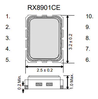
RX4901CE 外形尺寸 Unit: mm
Pin | Connection | ||
Option A | Option B | ||
1 | VDD | ||
2 | VOUT | ||
3 | VBAT | ||
4 | FOUT | EVIN3 | |
5 | SCL | ||
6 | EVIN1 | ||
7 | SDA | ||
8 | /INT | ||
9 | GND | ||
10 | EVIN2 | ||
RX4901CE 引脚功能
Signal Name | I / O | Function |
EVIN1,2,3 | Input | External event input pins. Detectable even in Backup mode. Pull-up and pull-down is configurable by the resisters. |
SCL | Input | Serial clock input pin |
SDA | Input / Output | Serial data input and output pin |
FOUT | Output | Frequency output pin (CMOS). 32.768 kHz (default), 1024 Hz or 1 Hz clock output is selectable. This pin can be switched to the wakeup timer interrupt output (CMOS) |
/INT | Output | Interrupt output pin (N-ch. open drain). The wakeup timer, time update, alarm, and/or event detection interrupt signals can be selected to output from this pin. When two or more signals are selected, they are NORed before being output. This pin is effective even in Backup mode. |
VDD | - | Power-supply pin |
VOUT | - | Internal operating voltage output pin Connect a 1.0 µF bypass capacitor to this pin. |
VBAT | - | Backup power supply pin Connect a backup power supply such as a large-size capacitor, secondary battery, or primary battery. The operating power voltage is supplied from this pin to the internal circuits in Backup mode. |
GND | - | Ground pin |
RX4901CE 规格
Recommended Operating Conditions
Item | Symbol | Condition | Min. | Typ. | Max. | unit |
Operating voltage | VDD | - | 1.6 | 3.0 | 5.5 | V |
Clock supply voltage | VCLK | - | 1.1 | 3.0 | 5.5 | V |
Operating Temperature | Ta | - | -40 | +25 | +105 | °C |
VDD detection voltage | -VDET1 | VDD, Fall | 1.35 | 1.45 | 1.55 | V |
Frequency Characteristics
Item | Symbol | Condition | Min. | Typ. | Max. | unit | |
Frequency tolerance | Df / f | XS | Ta = -40 to +85°C | -3 | - | +3 | ´ 10-6 |
Ta = -40 to +105°C | -5 | - | +5 | ||||
XB | Ta = -40 to +85°C | -5 | - | +5 | |||
Ta = -40 to +105°C | -8 | - | +8 | ||||
start-up time | tSTA | Ta = +25°C VDD = 1.6V~ 5.5V | - | 0.5 | 1.0 | s | |
Current consumption Ta = -40°C to +105°C
Item | Symbol | Condition | Min. | Typ. | Max. | unit |
IDD | IBAT | VBAT = 3.0 V, /INT= Hi-Z, FOUT: Output OFF (Hi-Z), Temperature compensation interval: 2 s, FSEL1= FSEL0 = 1, INIEN = 1, CHGEN = 0, SCL=SDA=L | - | 240 | 1500 | nA |
I32k | VDD = 3.0 V, /INT= Hi-Z, FOUT: 32 kHz output, CL = 0 pF, Temperature compensation interval: 2 s, FSEL1 = FSEL0 = 1, INIEN = 1, CHGEN = 0, SCL=SDA=H | - | 1.0 | 3.0 | mA |
Option
I/F | Option | EVIN pin Number | /INTpin Number | FOUT | Number of time stamps recorded by EVIN terminal trigge | |
FIFO Mode | Direct Mode | |||||
I2C | A | 2 | 1 | Yes | 32 times | 22 times |
B | 3 | 1 | - | 32 times | 22 times | |
型号 | 料号 | 封装 | MOQ |
RX8901CE XS A0 | X1B000481000115 | 3.2 x 2.5 x 1.0 | 2000PCS/REEL |
RX8901CE XB A0 | X1B000481000215 | 3.2 x 2.5 x 1.0 | 2000PCS/REEL |
RX8901CE XS B0 | X1B000481000315 | 3.2 x 2.5 x 1.0 | 2000PCS/REEL |
RX8901CE XB B0 | X1B000481000415 | 3.2 x 2.5 x 1.0 | 2000PCS/REEL |
Product Name RX8901CE XS A0
RX8901CE XB A0
RX8901CE XS B0
RX8901CE XB B0
(Standard form) ① ② ③ ④ ⑤
① Model ② Package type (CE : 3.2 x 2.5 x 1.0 mm Size)
③ Frequency tolerance (Exclude offset)
XS : ±3.0 x 10⁻⁶ / -40 ºC to +85 ºC (Monthly rate: ±8 seconds)
: ±5.0 x 10⁻⁶ / +85 ºC to +105 ºC (Monthly rate: ±13.2 seconds)
XB : ±5.0 x 10⁻⁶ / -40 ºC to +85 ºC (Monthly rate: ±13.2 seconds)
: ±8.0 x 10⁻⁶ / +85 ºC to +105 ºC (Monthly rate: ±21 seconds)
④ Pin Option
A: Option A
B: Option B
⑤ Reset output function
0: No /RST pin
8: With /RST pin (VDD drop detection voltage:+2.4V Type)
Product Number
RX8901CE XS A0 X1B000481000115
RX8901CE XB A0 X1B000481000215
RX8901CE XS B0 X1B000481000315
RX8901CE XB B0 X1B000481000415
① ② ③ ④ ⑤
① Crystal devices ② Model
③ Pb free code(1 or 2: EU RoHS compliant / Terminal plating : Sn)
④ Detail specifications ⑤ Packing (CE Standard 15: 2000pcs/Reel)
RX8901CE Footprint (Recommended)
RX8901CE
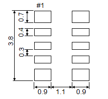
(Unit: mm)
为保持稳定运行,需提供一个 0.1uF 的旁路电容,在尽可能靠近晶体产品电源端子的位置(Vcc - GND 之间)。
 在线咨询
在线咨询
 微信服务
微信服务