
高稳定性实时时钟芯片(I2C 总线)
工作电压范围:1.70V 至 5.5V
用于计时的宽电压:1.15V 至 5.5V
多种检测功能:晶振停止检测功能
低备用电流:0.48μA / 3V(典型值)
32.768kHz频率输出功能
RX-8025SA / RX-8025NB: 爱普生(EPSON) 高稳定性实时时钟芯片(I2C 总线)
完整型号:
型号 | 料号 | 封装 | MOQ |
RX-8025SA AA | Q41802552000100 | SOP-14 | 1000PCS/REEL |
RX-8025SA AC | Q41802551000200 | SOP-14 | 1000PCS/REEL |
RX-8025NB AA | Q41802592000100 | SON-22 | 1000PCS/REEL |
RX-8025NB AC | Q41802592000200 | SON-22 | 1000PCS/REEL |
• 内置32.768kHz晶体单元
为高精度调整频率 (±5×10⁻⁶ / Ta=+25°C)
• 接口类型
I2C 总线接口 (400kHz)
• 工作电压范围
1.70V 至 5.5V
• 用于计时的宽电压
1.15V 至 5.5V
• 多种检测功能
晶振停止检测功能
• 低备用电流
0.48µA / 3V(典型值)
• 32.768kHz频率输出功能
带 OE 引脚的 C-MOS 输出
• 各种功能包括全日历、双重闹钟、定期中断
• *I2C-Bus 是 NXP Semiconductors 的商标
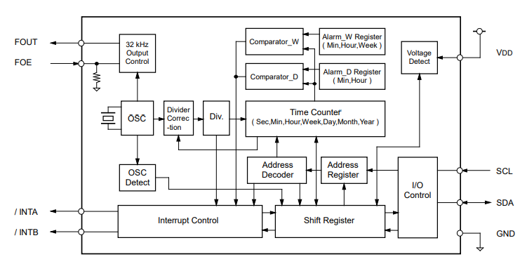
该模块是一个符合 I2C 总线接口的实时时钟,其中包括一个 32.768-kHz 石英振荡器,该振荡器已针对高精度进行了调整。该模块除了提供产生六种中断的功能、双重报警功能、振荡停止检测功能(用于确定上电时是否存在有效内部数据)和电源电压监控功能外,该模块还包括一个数字时钟精度调节功能,可用于设置各种精度等级。
由于内部振荡电路以恒定电压驱动,32.768-kHz 时钟输出稳定且自由电压波动的影响。
这种在一个 SMT 封装中实现多种功能非常适合从蜂窝网络等各种蜂窝电话到 PDA 和其他小型电子设备。
•内置 32.768 kHz 晶体单元:为高精度调整频率 (± 5 ×10⁻⁶ / Ta = +25 °C)
•接口类型:I2 C-Bus 接口 (400 kHz)
•工作电压范围:1.70 V 至 5.5 V
•用于计时的宽电压:1.15 V 至 5.5 V
•各种检测功能:例如,振荡停止检测功能
•低备用电流:0.48 µA / 3 V (Typ.)
•32.768 kHz 频率输出功能:C-MOS 输出与OE 引脚。
•各种功能包括全日历、双重闹钟、周期性中断。
• 特征
• 内置32.768 kHz 晶体单元
• 为高精度调整频率。 ( ± 5 ×10⁻⁶ / Ta = +25 °C ) ( 相当于 ±13 秒的月偏差)
• 多种检测功能
• 电源电压监控功能(可选择检测阈值)
• 停止检测功能
• 上电复位检测功能
• 报警功能和周期性中断功能
• 周期性中断输出。
• 双报警功能。(星期几,时,分)(月,日,时,分)
Recommend Operating Conditions
Item | Symbol | Condition | Min. | Typ. | Max. | Unit |
Power voltage | VDD | - | 1.7 | 3.0 | 5.5 | V |
Clock voltage | VCLK | - | 1.15 | 3.0 | 5.5 | V |
Operating temperature | TOPR | - | -40 | +25 | +85 | °C |
Frequency characteristics
Item | Symbol | Condition | Rating | Unit |
Frequency tolerance | Δ f/f | Ta=+25°C | AA: 5±5 *1) | ×10-6 |
Oscillation start-up time | tSTA | Ta=+25°C | 1 Max. | s |
Frequency voltage characteristics | f/V | Ta=+25°C | ±1 Max. | ×10-6 |
*1) 2) Equivalent to ±13 seconds of monthly deviation (excluding offset).
Current consumption characteristics Ta=-40°C to +85°C
Item | Symbol | Conditions | Min. | Typ. | Max. | Unit | |
Current Consumption | lBK | fSCL=0Hz | VDD=5V | - | 0.60 | 1.80 | µA |
VDD=3V | - | 0.48 | 1.20 | ||||
l32k | fSCL=0Hz | VDD=5.5V | - | 3.0 | 6.5 | µA | |
Power supply detection voltage Ta=-30°C to +70°C
Item | Symbol | Condition | Min. | Typ. | Max. | Unit |
High-voltage mode | VDETH | VDD pin | 1.90 | 2.10 | 2.30 | V |
Low-voltage mode | VDETL | VDD pin | 1.15 | 1.30 | 1.45 | V |
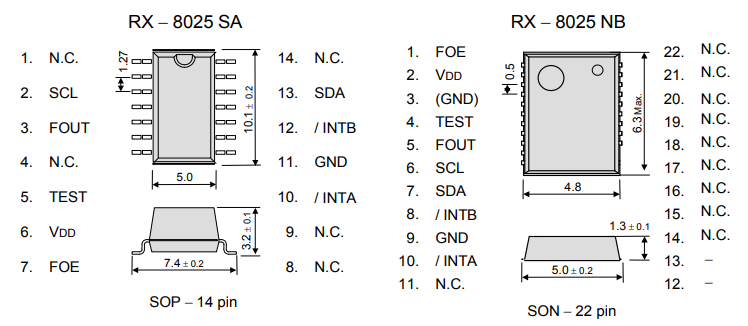
引脚功能
Signal | I / O | Function | ||||||||||||||||||||||||
SCL | I | This is the serial clock input pin for I2C communications. Data input and output across the SDA pin is synchronized with this pin's clock signal. Up to 5.5 V can be used for this input, regardless of the power supply voltage. | ||||||||||||||||||||||||
SDA | I/O | This pin's signal is used for input and output of address, data, and ACK bits, synchronized with the serial clock used for I2C communications. | ||||||||||||||||||||||||
FOUT | O | FOUT terminal is 32.768 kHz clock output terminal (C-MOS) that output control is possible. FOE terminal is the input terminal controlling the output of FOUT pin with /CLEN1 and /CLEN2 bit. The output of FOUT terminal stops when /CLEN1bit and /CLEN2 bit both sets to "1". FOUT output stops when FOE is Low or OPEN. Status of FOUT output stopped is " L ". ∗The logic table.
' Χ ' Don't care. FOE terminal had pull-down resistor built-in and input voltage is possible regardless of power supply voltage to 5.5 V. | ||||||||||||||||||||||||
FOE | I | |||||||||||||||||||||||||
/INTA | O | This interrupt output A pin is an N-ch open drain output. It outputs alarm interrupts (Alarm_D) and periodic interrupts. | ||||||||||||||||||||||||
/INTB | O | This interrupt output B pin is an N-ch open drain output. It outputs alarm interrupts (Alarm_W). | ||||||||||||||||||||||||
TEST | - | This pin is used by the manufacturer for testing. Do not connect externally | ||||||||||||||||||||||||
VDD | - | This pin is connected to a positive power supply. | ||||||||||||||||||||||||
GND | - | This pin is connected to a ground. | ||||||||||||||||||||||||
(GND) | - | This pin has the same voltage level as GND. Do not connect externally. | ||||||||||||||||||||||||
N.C. | - | This pin is not connected to the internal IC. However, note with caution that the RX-8025NB's N.C. pins (pins 14 to 22) are interconnected via the internal frame. Leave N.C. pins open or connect them to GND or VDD. |
注意:务必在 VDD 和 GND 之间连接一个额定值至少为 0.1 µF 的旁路电容。
型号 | 料号 | 封装 | MOQ |
RX-8025SA AA | Q41802552000100 | SOP-14 | 1000PCS/REEL |
RX-8025SA AC | Q41802551000200 | SOP-14 | 1000PCS/REEL |
RX-8025NB AA | Q41802592000100 | SON-22 | 1000PCS/REEL |
RX-8025NB AC | Q41802592000200 | SON-22 | 1000PCS/REEL |
Product Name RX-8025SA □
(Standard form) ① ② ③
① Model ② Package type (SA:SOP-14 pin;NB:SON-22 pin)
③ Frequency tolerance (Exclude offset)
AA: 5±5.0 x 10⁻⁶ (Equivalent to ± 13 seconds of monthly deviation) @ +25°C
AC: 0±5.0 x 10⁻⁶ (Equivalent to ± 13 seconds of monthly deviation) @ +25°C
Product Number
RX-8025SA AA Q41802552000100
RX-8025SA AC Q41802551000200
RX-8025NB AA Q41802592000100
RX-8025NB AC Q41802592000200
① ② ③ ④ ⑤
① Crystal devices ② Model
③ Pb free code(1 or 2: EU RoHS compliant / Terminal plating : Sn)
④ Detail specifications ⑤ Packaging (1000pcs/Reel)
1. RX-8025SA
2. RX-8025NB
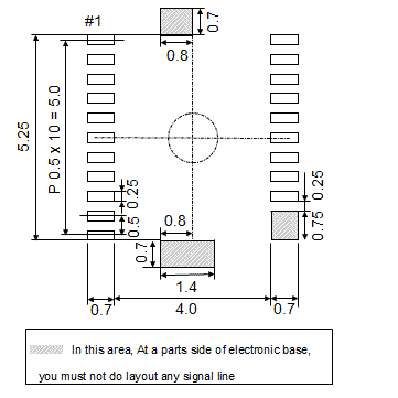
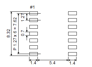
(Unit: mm)
为保持稳定运行,需提供一个 0.1uF 的旁路电容,在尽可能靠近晶体产品电源端子的位置(Vcc - GND 之间)。
 在线咨询
在线咨询
 微信服务
微信服务