实时时钟芯片,RTC,内置调频32.768 kHz晶体单元和DTCXO
I2C 总线接口 (400 kHz)
接口电压范围:1.8 V 至 5.5 V、温度补偿电压范围:2.2 V 至 5.5 V
宽计时器电压范围:1.6 V 至 5.5 V
32.768 kHz频率输出功能:C-MOS输出带控制Pin
各种功能包括完整的日历、闹钟、定时器
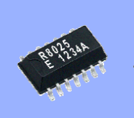
RX-8025T:爱普生(EPSON) RTC 实时时钟芯片
RX-8025T 内置32.768 kHz-DTCXO,高稳定性,I2C 总线接口实时时钟模块
完整型号:
RX-8025T UB (X1B000281000400)
RX-8025T UC (X1B000281000500)
RX-8025T 特征
• 内置调频32.768 kHz晶体单元和DTCXO。
• 接口类型:I2C 总线接口 (400 kHz)
• 接口电压范围:1.8 V 至 5.5 V
• 温度补偿电压范围:2.2 V 至 5.5 V
• 宽计时器电压范围:1.6 V 至 5.5 V
• 32.768 kHz频率输出功能:C-MOS输出带控制Pin
• 各种功能包括完整的日历、闹钟、定时器。
* I2C-Bus 是 NXP Semiconductors 的商标
• 高稳定性
• RX-8025T UA
± 1.9 x 10⁻⁶ / 0ºC 至 +40 ºC (相当于 5 秒的月偏差)
± 3.4 x 10⁻⁶ / -40 ºC 至 +85 ºC (相当于 9 秒的月偏差)
• RX-8025T UB
± 3.8 x 10⁻⁶ / 0ºC 至 +50 ºC (相当于 10 秒的月偏差)
± 5.0 x 10⁻⁶ / -40 ºC 至 +85 ºC (相当于 13 秒的月偏差)
• RX-8025T UC
± 3.8 x 10⁻⁶ / 0ºC 至 +50 ºC (相当于 10 秒的月偏差)
± 5.0 x 10⁻⁶ / -30 ºC 至 +70 ºC (相当于 13 秒的月偏差)
• 32.768 kHz 频率输出功能
• FOUT 引脚输出(C-MOS 输出),CL=30 pF
• 输出可选< 32.768 kHz、1024 Hz、1 Hz >
• 各种中断
• 定时器功能可以在两者之间设置1/ 4096 秒和 255 分钟。
• 闹钟功能可以设置为星期几、星期几、小时或分钟。
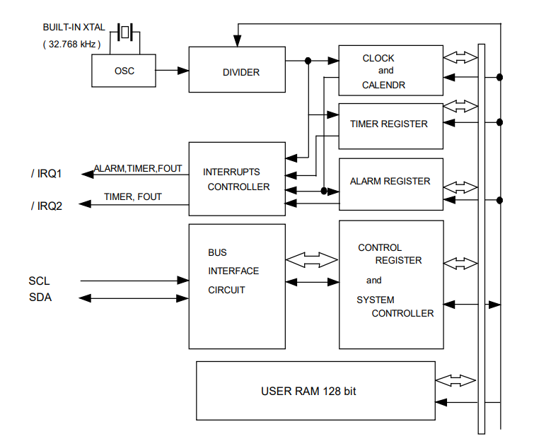
RX-8025T 系统框图
RX-8025T 引脚连接
RX-8025T 引脚功能
Signal name | I/O | Function |
T1 | Input | * Use by the manufacture for testing. ( Do not connect exterally.) |
SCL | Input | This is the serial clock input pin for I'C Bus communications. |
FOUT | Output | This is the C-MOS output pin with output control provided via the FOE pin. When FOE = "H" (high level), this pin outputs a 32.768 kHz signal. When output is stopped, the FOUT pin = "Hi-Z"( high impedance). |
TEST | Input | * Use by the manufacture for testing. ( Do not connect externally) |
VDD | - | This pin is connected to a positive power supply. |
FOE | Input | This is an input pin used to control the output mode of the FOUT pin. When this pin's level is high, the FOUT pin is in output mode. When it is low, output via the FOUT pin is stopped. |
1 INT | Output | This pins is used to output alarm signals, timer signals, time update signals, and other signals. This pin is an open drain pin |
GND | - | This pin is connected to a ground. |
T2 | - | * Use by the manufacture for testing. ( Do not connect externally) |
SDA | I/O | This pin's signal is used for input and_ output of address, data, and ACK bits, synchronized with the serial clock used for I'C communications. Since the SDA pin is an N-ch open drain pin during output, be sure to connect a suitable pull-up resistance relative to the signal line capacity. |
N.C. | - | This pin is not connected to the internal IC. Leave N.C. pins open or connect them to GND or VDD. |
注意:务必在 VDD 和 GND 之间连接一个额定值至少为 0.1 μF 的旁路电容。
RX-8025T 包装信息
型号 | 料号 | 工作温度范围 | 包装 |
RX-8025T UB | X1B000281000400 | -40 ºC to +85 ºC | 1000pcs/Reel |
RX-8025T UC | X1B000281000500 | -30 ºC to +70 ºC | 1000pcs/Reel |
 在线咨询
在线咨询
 微信服务
微信服务